 Log In
Search




 Open Access
 yanrongguo@usst.edu.cn
Rongguo Yan, School of Health Science and Engineering, University of Shanghai for Science and Technology, No. 516, Jun Gong Road, Yangpu District, Shanghai 200093, China. E-mail: yanrongguo@usst.edu.cn.
Received November 18, 2025; Accepted January 16, 2026; Published June 3, 2026
Established potential displacement-charge-voltage relation for polyvinylidene fluoride by means of the first-order piezoelectric equation.
Applied COMSOL multilayer shell model and multiphysics coupling for calculating the interlayer stress and electric displacement field.
Structurally explored how changes to structural parameters impacted sensor performance through the control variable method.
Open Accessyanrongguo@usst.edu.cnRongguo Yan, School of Health Science and Engineering, University of Shanghai for Science and Technology, No. 516, Jun Gong Road, Yangpu District, Shanghai 200093, China. E-mail: yanrongguo@usst.edu.cn.
Received November 18, 2025; Accepted January 16, 2026; Published June 3, 2026
Established potential displacement-charge-voltage relation for polyvinylidene fluoride by means of the first-order piezoelectric equation.
Applied COMSOL multilayer shell model and multiphysics coupling for calculating the interlayer stress and electric displacement field.
Structurally explored how changes to structural parameters impacted sensor performance through the control variable method.
Objective: Accurately capturing signals from healthcare devices worn on the body is vital for health monitoring, a field of growing interest. A flexible polyvinylidene fluoride (PVDF)-based piezoelectric sensor has been chosen for wearable applications. This study aims to optimize PVDF sensor performance by focusing on structural design. Methods: According to piezoelectric theory, this paper presents a mathematical expression system centered on the first-order piezoelectric equation, which describes the relationship between the electric displacement, the quantity of charge, and the output voltage of the PVDF film under strain. The study focuses on the features of weak physiological signals in the human body to establish a multi-layer shell structure finite element model using COMSOL Multiphysics. The analysis covers the electric displacement field mode, output charge, electric potential, and uniformity of stress distribution. We systematically investigated the impact of PVDF piezoelectric layer area, shape, thickness, and encapsulation materials on sensor performance using the controlled variable method. Results: As the area increases, the sensitivity and stress uniformity improve. Rectangular shapes exhibit more uniform stress distribution than circular shapes, and raising the aspect ratio within a certain range further enhances stress uniformity while maintaining comparable sensitivity. Increasing the thickness of the piezoelectric layer raises the electrical potential. Flexible encapsulation materials can provide higher sensitivity than rigid materials but are more susceptible to stress concentration. Conclusion: This paper finds the best structural form and parameter adjustment range of the PVDF sensor, which can provide a theoretical basis and numerical references for designing high-performance wearable sensors.
Keywords: Polyvinylidene fluoride flexible sensor, Wearable sensing technology, COMSOL simulation, Piezoelectric effect
Due to the increasing social demand for daily health monitoring, wearable sensing technology is widely recognized and is gradually becoming a major direction of development in medical diagnosis. Among the different types of wearable sensors, piezoelectric, piezoresistive, capacitive, and triboelectric sensors have the best application prospects [1, 2]. Piezoelectric materials have obvious self-powered characteristics and low energy consumption, which can meet the needs of long-term health monitoring, exercise physiology parameter monitoring, and non-invasive monitoring for chronic disease patients [3-5]. Sensors made with piezoelectric material, as shown in Figure 1A, can convert mechanical energy into electrical energy via the piezoelectric effect when subjected to mechanical force [6, 7]. Traditional piezoelectric materials mostly use rigid ceramics such as lead zirconate titanate and lead titanate. Though highly sensitive, these devices are fragile, and there is a biocompatibility problem that affects comfort; results can also be inaccurate if they do not adhere properly [8, 9]. To tackle these shortcomings, flexible sensors have become an important direction for development. In 1969, Kawai discovered the piezoelectricity of polyvinylidene fluoride (PVDF), whose polarized film has a piezoelectric coefficient as high as 6-7 pC/N—ten times that of any other polymer [10]. As can be seen from Figure 1B, PVDF is becoming a popular material for flexible wearable sensors because of its good piezoelectric property, flexibility, biocompatibility, and cost-effectiveness [11-13].
In recent years, a lot of research has proved that PVDF can be used for wearable applications. Ghosh et al. developed a Pt-PVDF piezoelectric nanogenerator that served as a static strain-sensitive wearable tactile sensor [14]. Yang et al. created a self-powered, breathable, high-performance flexible wearable sensor using an electrospun polarized PVDF-barium titanate membrane and a Ni fabric electrode [15]. The physiological signals of the human body are mostly weak and easily interfered with, so high sensor sensitivity is required. To improve the piezoelectric properties of PVDF, most studies aim at increasing the β-phase content [16]. Electrospinning is a commonly used method. He et al. found that by controlling process, solution, and environmental parameters, PVDF molecular dipoles can be oriented to significantly increase the β-phase fraction and crystallinity [17]. Adding nanofillers can also significantly increase the proportion of β-phase. Parangusan et al. noticed that increasing the amount of Co-ZnO nanofillers in the PVDF-hexafluoropropylene matrix raised the quantity of crystalline β-phase, leading to a dramatic increase in the output voltage of the flexible nanogenerator [18]. Islam et al. used 3D printing to fabricate PVDF-MoS2 composites and achieved in-situ dipole alignment through shear stress, which increased the piezoelectric coefficient eightfold relative to pure PVDF, correlating with an increased β-phase volume fraction [19]. Structural optimization has also been studied. Liu et al. built a multiscale porous structure, as shown in Figure 1C, and combined it with corona polarization to produce an electret effect and improve sensor performance [20]. Xue et al. designed a cylindrical arch structure to optimize PVDF film deformation and enhance the sensor’s signal acquisition capacity [21]. Kim et al. developed an air-expansion approach to create dome-shaped PVDF films (Figure 1D) and fabricated a dome-shaped 4×4 array tactile sensor, finding that dome-shaped sensors are more sensitive than planar ones [22]. Yan et al. built a basic PVDF simulation model and changed the length, width, and height of the PVDF structure to study the effect of structural parameters on sensor sensitivity, as shown in the stress distribution results in Figure 1E [23]. Wang et al. proposed external strategies like electrode design and stress modification, offering new ways to improve PVDF sensor performance [24]. These studies provide practical technical pathways for developing the next generation of comfortable and efficient wearable health monitoring devices.

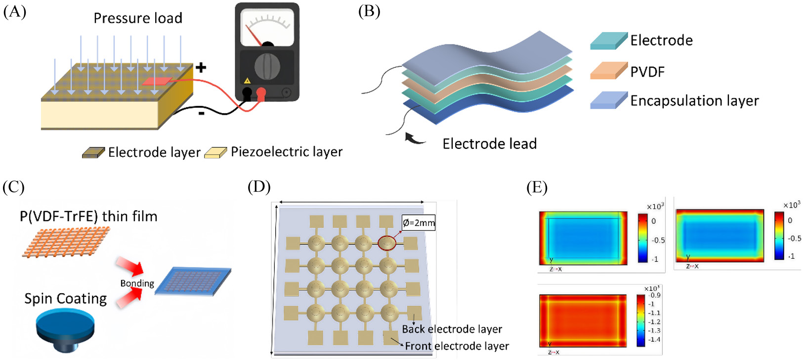
Figure 1. Schematic diagram related to the development of PVDF sensors. (A) Schematic of the piezoelectric sensor principle; (B) Flexural characteristics of PVDF piezoelectric film; (C) Preparation of multi-scale porous P(VDF-TrFE) film; (D) Structure of a 4×4 array tactile sensor; (E) Stress distribution along the length, width, and height of the PVDF film. PVDF, polyvinylidene fluoride; P(VDF-TrFE), poly(vinylidenefluoride‑trifluoroethylene).
2.1 Piezoelectric effect of PVDF film sensors
The finding of the piezoelectric effect is traced back to when the Curie brothers first found an unusual electromechanical phenomenon while working with a quartz crystal. When an electric field is applied to the crystal, it deforms; conversely, when a mechanical load is applied, surface charges are generated. As for the features of PVDF thin-film sensors, their general structure is a layered thin film. The thickness direction (usually the 3-axis direction) is the polarization direction, with electrodes deposited on the top and bottom surfaces. When subjected to a load, charge separation along the polarization direction generates equal but opposite charges on the upper and lower surfaces. This is known as the direct piezoelectric effect. As shown in Figure 2, polarization occurs along the thickness direction; applying a load results in positive charge accumulation on the upper surface and negative charge on the lower surface.
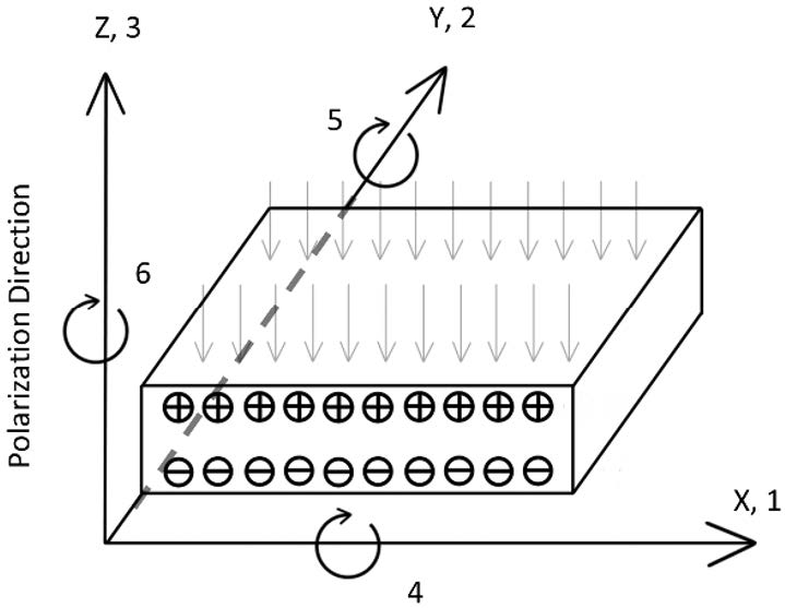
Figure 2. Schematic of the positive piezoelectric effect in PVDF film. PVDF, polyvinylidene fluoride.
To quantitatively characterize this electromechanical conversion mechanism, a comprehensive mathematical framework must be established. Under the assumption of linear material response, this can be expressed via matrix equations, typically employing the first-order piezoelectric equation [25-27]:

Where D (C/m2) is the electric displacement vector, x is the strain tensor; E (V/m) is the electric field intensity vector, X (Pa) is the stress tensor; εX represents the dielectric constant matrix under constant stress, sE represents the elastic modulus matrix under constant electric field, d denotes the piezoelectric strain coefficient matrix, and dT is the transpose of d. This equation describes the bidirectional energy conversion mechanism of piezoelectric materials.
When PVDF is applied to thin-film sensors, no external electric field is present. Under such conditions, the general equation (1) reduces to the following form [26]:

Expanding equation (2) using Voigt notation yields [27]:
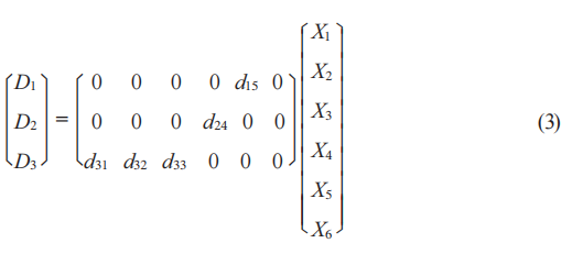
In the equation, D1, D2, D3 denote the components of the electric displacement vector, describing the charge density distribution along the corresponding axes; X1, X2, X3 denote the normal stress components, characterizing tensile or compressive stress along each principal direction; X4, X5, X6 denote the shear stress components, describing the in-plane shear deformation forces acting on the material.
The thickness of PVDF film sensors is far smaller than their in-plane dimensions, making direct measurement of in-plane displacement components D1 and D2 challenging. Conversely, D3 can be directly acquired via the upper and lower electrodes, representing an effective physical quantity directly correlated with the sensor’s output signal. Considering measurement feasibility and practical application requirements, we focus on D3 and simplify it as [23]:

The surface charge density σ=D3 on the electrode plane, and the total accumulated surface charge Q can be expressed as:

From a circuit standpoint, the PVDF film structure can be seen as a parallel-plate capacitor, whose capacitance C is a function of the dielectric properties and dimensions of the material:

Where ε0 is the vacuum permittivity, εr is the relative permittivity of PVDF, A is the film area, and h is the film thickness. This yields an expression for the output voltage U across the electrodes:

According to the piezoelectric mechanism, structural configuration, and mathematical modeling of the PVDF film sensor, a clear relationship among the electrical displacement, accumulated charge, and output voltage has been established.
2.2 COMSOL simulation preparation
2.2.1 Constitutive equation simulation implementation
To convert the above theoretical model into a practical simulation method in COMSOL Multiphysics, we need to specify the form of the governing equations to be implemented. For applications dominated by the direct piezoelectric effect, like PVDF thin-film sensor, the “strain-charge” formulation should be chosen. The fundamental governing system consists of three physical equations [28, 29].
Dynamic equilibrium equation:
Where ρ is the density of PVDF,  is the acceleration vector, ∇·S is the divergence of the stress tensor S, and Fv is the volume force vector. This equation describes the mechanical vibration response of the film and serves as the foundation for analyzing deformation due to load.
Electrostatic Gauss’s law:

Where ∇·D is the divergence of the electric displacement vector D and ρv is the free charge density. This equation governs how the electric displacement field distributes in space with respect to free charges.
Electromechanical coupling constitutive relations:

Where c is the elastic stiffness tensor, e is the piezoelectric stress constant tensor, and ε is the total strain tensor. This is the basic system of equations for electromagnetic coupling. The former refers to the mechanical response “strain → stress”, whereas the latter one is the piezoelectric effect “strain → electric displacement”. This creates a direct correlation between PVDF film deformation and electrical signal output, thereby transforming mechanical load into an electrical quantity.
According to the derivation and theory of the above piezoelectric equation, the material parameters of PVDF must be defined to establish a successful simulation model in COMSOL. These parameters include density, elastic modulus matrix, piezoelectric strain constant matrix, and free relative permittivity. They govern PVDF’s electromechanical response characteristics, and must satisfy the complete tensor description for an orthotropic anisotropic material [28]. The selected parameter values are shown in Table 1.

2.2.2 Construction of the multilayer shell model
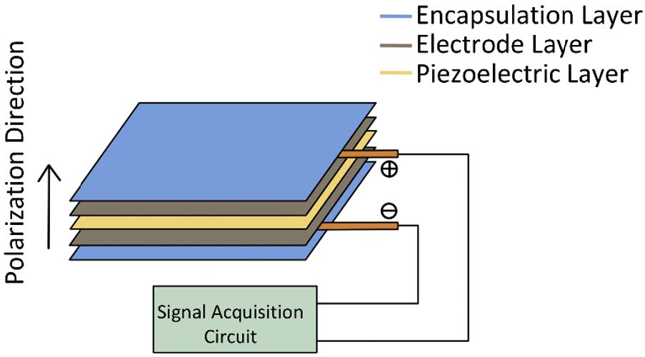
PVDF sensors typically feature a multilayer planar structure. As shown in Figure 3, the configuration comprises five layers: upper and lower encapsulation layers, a PVDF piezoelectric layer, and two intermediate electrode layers. The electrode layers serve to conduct charge [11, 30]. Given that this study focuses on the influence of piezoelectric-layer structural parameters and encapsulation-material selection on sensor performance, and considering that the electrode-layer thickness is extremely thin (typically 6 μm), its effect on the overall stress distribution can be neglected. The simulation model can thus be simplified to a three-layer structure consisting of the upper and lower encapsulation layers with the PVDF piezoelectric layer in between.
2.2.3 Sensor design parameters and boundary condition settings
In this study, it is found that area, shape, thickness and encapsulation material of the sensor’s piezoelectric layer are the most important parameters. Area is chosen between 1 and 25 cm2. An excessively small area hampers the capture of broad-range signals like breathing and body motion, while an overly large area could cause non-uniform strain because of insufficient bonding space and increase wearing discomfort. Common sensor shapes include circular and rectangular geometries. Several standard PVDF thicknesses are available: 28 μm, 52 μm, and 110 μm, among others. Thinner films (e.g., 28 μm) offer greater comfort, whereas thicker ones (e.g., 110 μm) tend to provide higher sensitivity. Common encapsulation materials are polyethylene terephthalate (PET), polydimethylsiloxane (PDMS), nylon, polyimide (PI), and polyvinyl alcohol (PVA) [1]. Different encapsulation materials can significantly affect sensor performance. The material parameters used for the five encapsulation materials in this study are listed in Table 2.
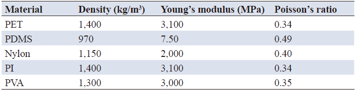
Note: PET, polyethylene terephthalate; PDMS, polydimethylsiloxane; PI, polyimide; PVA, polyvinyl alcohol.
2.3 COMSOL simulation workflow
After the above preparations are completed, the model can be built. First, select “Geometry” and draw rectangles or circles to make up a composite structure. Under “Materials”, add multilayer material. Assign PVDF to the middle layer and the chosen encapsulation material to the top and bottom layers. Parameters for each layer like its thickness, elastic modulus, Poisson’s ratio, and piezoelectric constant are then set. Finally, the “Layer Cross-Section Preview” and “Layer Stacking Pre-view” functions can be used to visualize the multilayer shell structure, as shown in Figure 4.
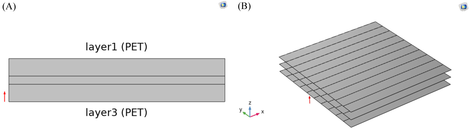
The model setup is completed and boundary conditions are applied. First, the “Multilayer Shell” and “Current in Multilayer Shell” physics interfaces are added to form the basis for multiphysics coupling. Under the “Multilayer Shell” node, the following features are added: “Piezoelectric Material”, “Fixed Constraint”, and “Surface Load”. For “Piezoelectric Material”, “Layer 2” is selected with the constitutive relationship set to “Strain-Charge”. The option “Maintain out-of-plane material orientation unchanged” is enabled to keep polarization aligned along the Z-axis. A “Fixed Constraint” is applied to “Layer 3” (upward direction). For “Surface Load”, “Downward on Layer 1” is chosen and a value of 1,000 Pa is entered. Under the “Current in Multilayer Shell” node, “Insulating Layer” and “Piezoelectric Layer” are added. “Layer 1” and “Layer 3” are assigned as “Insulating Layer”, while “Layer 2” is defined as the “Piezoelectric Layer”. If required, a “Ground” condition can be added under the “Piezoelectric Layer” node. When calculating surface potential and stress, “Layer 2-Layer 3” is set as grounded. The surface displacement field modulus and output charge are then computed. For charge-related outputs, both “Layer 1-Layer 2” and “Layer 2-Layer 3” interfaces are grounded.
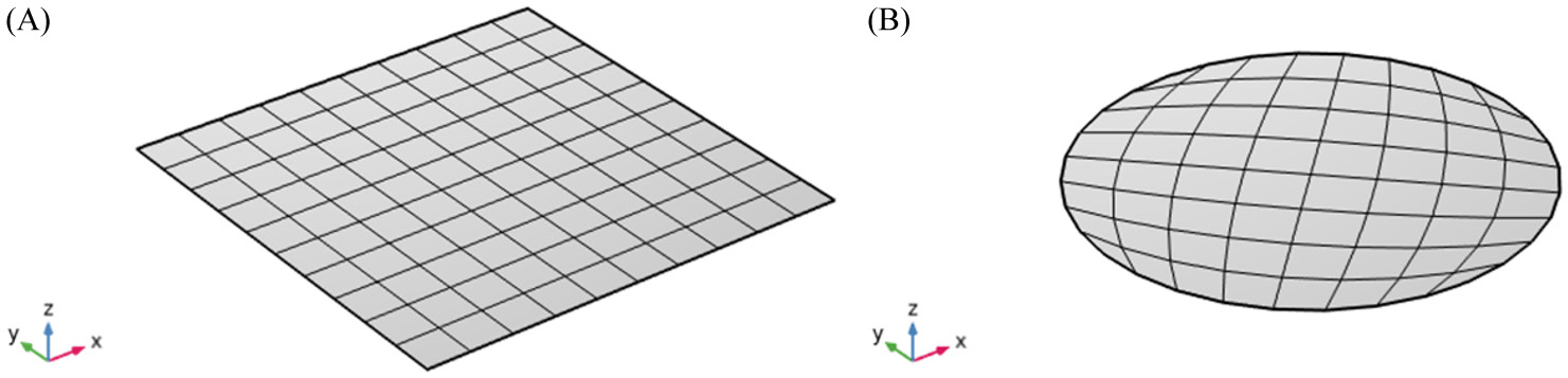
After applying the boundary conditions, the mesh is generated. Mesh quality is directly related to the accuracy of the simulation. In this study, a mapped mesh is used, as shown in Figure 5. Mapped meshing allows precise control of element size and distribution, resulting in high-quality, uniformly distributed elements [33].
3.1 Simulation results of the basic model
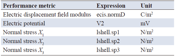
To prove the rationality of the simulation model and methodology, a basic sensor model is set up using 9 cm2 area, a 28 μm thickness and 60 μm thick PET encapsulating material. According to the “COMSOL simulation workflow” described above, the electric displacement field distribution (Figure 6A), electric potential distribution (Figure 6B), and stress distribution on the upper surface of the multilayer shell piezoelectric layer (Figure 6C) under static condition are obtained through COMSOL simulation. As shown in Figure 6A, under stress the piezoelectric layer has identical electric displacement field modulus on both the upper and lower surfaces. The arrow direction indicates the direction of the electric displacement field on the surface of the piezoelectric layer, which is generally downward. Near the edges, however, affected by the boundary of the multilayer shell and the material interface, the direction of the electric displacement field is not parallel to the electric field direction but has a certain deflection angle. As can be seen in Figure 6B, the potential of the top and bottom insulating layers remains constant. The lower surface of the piezoelectric layer is grounded, so its potential is almost 0 mV. On the upper side, polarization charges accumulate, creating a potential difference relative to the lower side, reaching up to 9.54 millivolts. Figure 6C shows a non-uniform stress distribution in the piezoelectric layer. Stress components in different directions exhibit distinct color gradients in the plane, with a pronounced difference between the edge and center regions. The average values of the surface electric displacement field modulus, output charge, electric potential, and stress components X1, X2, and X3 are summarized in Table 4.
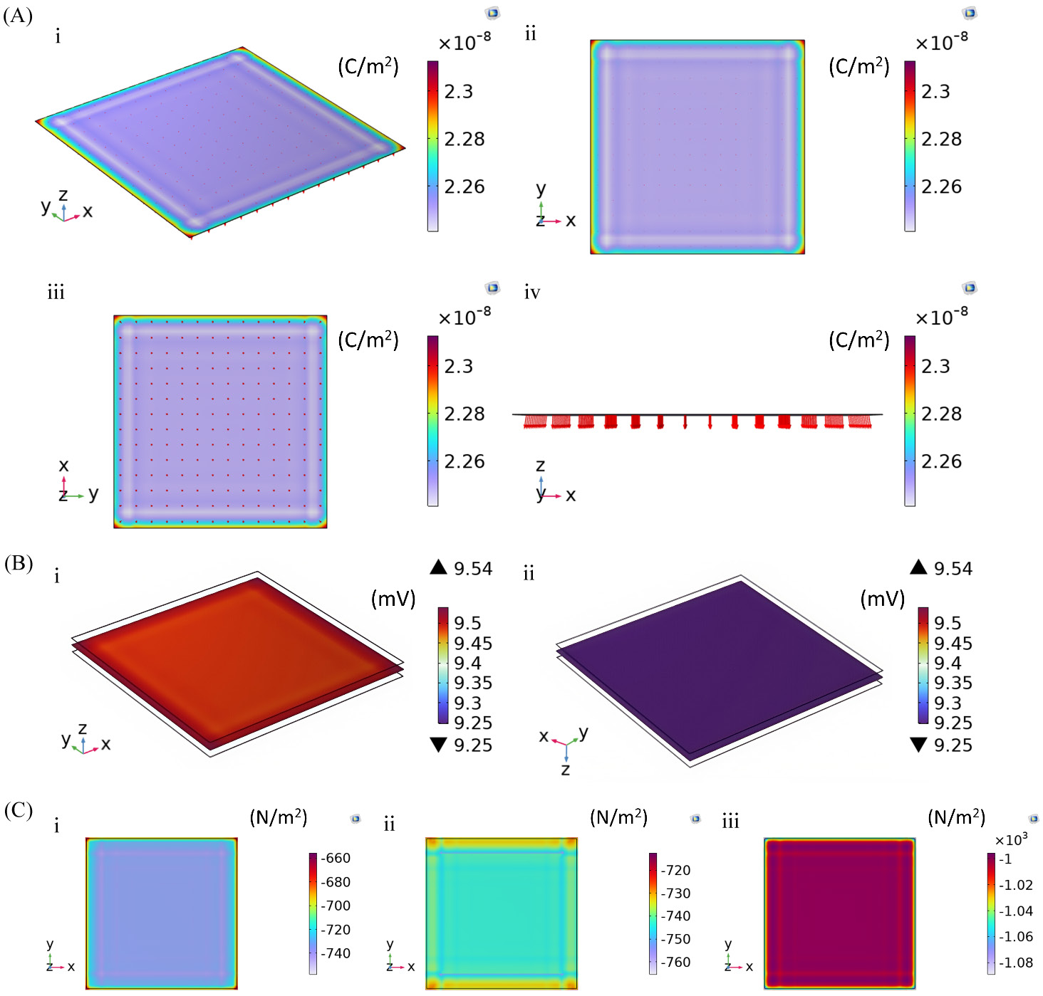
Figure 6. Simulation results for the base model. (A) Electric displacement field distribution of the multilayer shell piezoelectric layer: (i) Front view; (ii) Upper surface; (iii) Lower surface; (iv) Side view. (B) Electric potential distribution of the multilayer shell piezoelectric layer: (i) Upper surface; (ii) Lower surface. (C) Stress distribution on the upper surface of the multilayer shell piezoelectric layer: (i) Stress X1; (ii) Stress X2; (iii) Stress X3.

Substituting the simulated stress values X1, X2, X3 and piezoelectric constants into equation (4), the electric displacement field modulus is calculated as:

Compared with the simulated electric displacement field modulus of 2.253×10⁻⁸ C/m2, the calculation error rate is:

Using equations (5), (6), and (7), the calculated charge output is 20.547 pC and the potential is 9.335 mV, with relative errors of 1.29% and 0.45%, respectively—both below 5%. These results indicate that the simulation model accurately captures the coupling between the piezoelectric effect and the stress field, validating the model and analysis methodology.
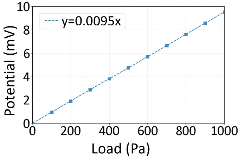
To analyze the linearity of the sensor under varying loads, the load was successively set to 0, 100, 200, 300, 400, 500, 600, 700, 800, 900, and 1,000 Pa. The surface potential of the piezoelectric layer was measured at each load step, yielding the results shown in Figure 7. A linear fit of upper surface potential versus load gives the relationship y=0.0095x, with R2=0.99. Indicating a very high degree of linear correlation between the sensor output and the applied external load.
3.2 Parameter optimization of multilayer shell structures
Based on the simulation results of the baseline model, sensitivity, stress distribution uniformity, and linearity are key metrics for evaluating sensor performance. Sensitivity is characterized by three indicators: the electric displacement field magnitude on the upper surface of the piezoelectric layer, the output charge quantity, and the electric potential. The electric displacement field pattern represents the charge generation capacity per unit stressed area, the output charge quantity represents the total charge output, and the electric potential represents the voltage signal strength formed by the accumulated charges [34, 35]. Stress distribution uniformity refers to the uniformity of the stress distribution on the upper surface of the piezoelectric layer under external load. Uniform stress distribution can ensure consistent piezoelectric conversion efficiency and help avoid the problems such as signal distortion, sensitivity change, and structural fatigue failure caused by concentrated stress. Maintaining uniform stress is therefore critical for sensor accuracy, stability and durability [36, 37]. Since the piezoelectric effect of this sensor is primarily determined by X1, X2, and X3, the uniformity of stress distribution can be quantified by calculating the standard deviation of these three components. A smaller standard deviation indicates more uniform distribution of stress in that direction and better overall sensor performance. Linearity shows the proportional connection between the output signal and the input load, which is important for ensuring measurement accuracy [34].
Based on the parameters outlined in Section 2.2.3 “Sensor design parameters and boundary condition settings”—namely piezoelectric-layer area, shape, thickness, and encapsulation material—an optimization strategy can be formulated. To evaluate the individual effect of each structural parameter on sensor performance, a controlled‑variable approach is adopted. This involves keeping all variables constant except the one under investigation. Simulations are conducted sequentially by varying the area, shape, thickness, and encapsulation material, while recording the corresponding changes in performance metrics. A comparative analysis of these results identifies the optimal range for each parameter, providing a quantitative basis for structural optimization of the sensor. Furthermore, subsequent simulations reveal that adjusting these structural parameters does not significantly alter the sensor’s linear characteristic, which remains consistently high. This confirms the stability of linearity within the current structural framework and establishes a reliable benchmark for subsequently optimizing sensitivity and evenness of the stress distribution.
3.2.1 Analysis of piezoelectric layer structure impact on sensor performance
To investigate the influence of area on sensor performance, the thin film area is changed according to the model in the Section 3.1 “Simulation results of basic model”, while keeping all other simulation conditions unchanged. Effects of different areas on sensor sensitivity and stress distribution are summarized in Table 5. As for the sensitivity, the electric displacement field modulus and the electric potential decrease only slightly as the area increased, while the output charge increase linearly with the area, as seen in the theoretical derivation in equation (5). For the stress distribution uniformity aspect, increasing the area greatly improves uniformity: the standard deviations of stress in the three directions decrease significantly with increasing area. This shows that a larger area distributes the load more broadly and reduces stress concentration. Overall, increasing the area benefits both sensitivity and stress distribution uniformity.

To explore the impact of sensor shape, a circular model and an equilateral rectangular model—each with an area of approximately 9 cm2 (radius =1.693 cm)—are simulated under identical conditions. The stress distribution of the circular piezoelectric layer is depicted in Figure 8, and the sensitivity and stress distribution results for both shapes are displayed in Table 6. A comparison of the stress distribution in Figure 8 with that of the rectangular layer in Figure 6C reveals stress concentration at the edges of both shapes. According to the color legend data, it can be known that the stress values in all three directions are higher for the circular layer and are more dispersed, indicating poorer stress uniformity in the circular geometry. Regarding sensitivity, Table 6 shows that the electric displacement field modulus and electric potential are nearly identical for both shapes, while the rectangular sensor has a slightly higher output charge. The overall differences are negligible, suggesting that shape change does not have a significant effect on the sensitivity of the piezoelectric conversion. In terms of stress distribution uniformity, the standard deviations of stress in all three directions are smaller for the rectangular sensor than for the circular sensor, by factors ranging from 1 to 8. This shows that under external loading, the circular sensor exhibits much poorer directional consistency in stress distribution and is more prone to issues such as local stress concentration.


Building upon the rectangular shape, the aspect ratio is varied to investigate its influence on sensitivity and stress distribution; the results are presented in Table 7. Concerning sensitivity, the modulus of the electric displacement field is constant across different aspect ratios. Both the output charge and the electric potential have a slight decreasing trend as the aspect ratio increases, although the numerical differences are minor. This means that changes in aspect ratio do not significantly affect the piezoelectric conversion sensitivity of the sensor. For the stress distribution uniformity, the standard deviations of stresses in three directions reduce continuously with increasing aspect ratios, with the most pronounced decrease found in X1. These results suggest that properly enhancing the aspect ratio improves the evenness of the stress distribution and helps mitigate local stress concentration.


3.2.2 Analysis of encapsulation material effects on sensor performance
To examine the influence of Encapsulation materials on sensor performance, multilayer shells using different materials are simulated under the same conditions. The results in Table 9 show the effect of encapsulation material on sensitivity and stress distribution.

In terms of sensitivity, sensors encapsulated with PET, PI, PVA, and nylon exhibit the identical values for the electric displacement field modulus, output charge, and electric potential. In contrast, PDMS encapsulation yields significantly higher values for these metrics. This difference is probably due to different Young’s moduli of the encapsulation materials. The data suggest that a lower Young’s modulus corresponds to higher sensitivity. Rigid materials such as PET, PI, PVA, and nylon impose more constraints on the mechanical deformation of the piezoelectric layer, restricting its strain response to external excitation and decreasing piezoelectric conversion efficiency. On the contrary, flexible PDMS exerts less constraint, maximizing the mechanical deformation of the piezoelectric layer. Under the same external excitation, a piezoelectric layer embedded in PDMS therefore produces a larger effective strain output.
As to the degree of stress distribution uniformity, the standard deviations of stresses in the three directions are in creasing successively for PET, PI, PVA and nylon encapsulation. This shows that among these materials, PET has the best stress distribution uniformity, and nylon gives the worst. However, for the PDMS encapsulation case, the standard deviations of stress in the X1 and X2 directions increase sharply, while only the X3 direction is comparable to other materials. This shows that the PDMS seriously degrades the uniformity of the stress distribution and is prone to the formation of local stress concentration. Rigid encapsulation materials undergo only limited deformation and can transmit external stress more uniformly to the piezoelectric layer. Their stiffness helps prevent large localized deformation in the piezoelectric layer, thereby lowering the risk of stress concentration. In contrast, flexible PDMS deforms non-uniformly. Under external loading, it not only transmits stress unevenly, but its own deformation can also induce uneven stress distribution among various parts of the piezoelectric layer, leading to pronounced localized stress concentration and an increase in stress standard deviation.
4.1 Reliability and rationality of the simulation model
This study uses a multi-layer shell structure finite element model built by COMSOL, and the experiment shows good validation accuracy. Theoretical calculations on the electric displacement field, output charge quantity, and electric potential all show less than 5% error during simulation, showing that the model is correct in simulating the piezoelectric effect and charge generation of PVDF film under stress. A strict controlled variable approach is used to build the simulation framework. All the simulations use the same boundary conditions, such as the size of the external load and the method of restricting sensors. This minimizes interference from confounding factors, allowing clear attribution of performance variations to the specific parameter being studied. Consequently, the approach provides a reliable basis for subsequent parameter optimization. Trends observed in the simulation data closely align with key aspects of mechanical transmission and piezoelectric theory. For instance, the variation in sensitivity with piezoelectric-layer thickness follows the theoretical piezoelectric equations. Concerning the encapsulation material, flexible PDMS has far more permissive deformations of the piezoelectric layer, leading to a larger effective strain release and significantly higher sensitivity metrics compared to rigid PET materials. But because it is prone to non-uniform deformation, the stress standard deviation in the X1 and X2 directions increases, which is in line with the stress-transmission characteristics of flexible materials [38]. The data show no logical contradictions or anomalous fluctuations, further verifying the reliability of the simulation results.
4.2 Influence of structural parameters on sensor performance
The influence of structural parameters on the performance of wearable sensors involves a compromise between “optimal performance” and “diversity of wearable applications”, achieved by adjusting stress transfer efficiency, material usage adaptability, and piezoelectric conversion. Wearable applications include motion posture monitoring, physiological signal collection, and human-computer interaction, which all have different requirements for sensor sensitivity, portability, and fit. Therefore, structural parameters must be tuned to balance general applicability with scenario-specific demands.
Increasing the sensor area distributes external loads more widely and reduces stress concentration, significantly lowering the standard deviations of stresses in all three directions. The output charge is proportional to the area, allowing simultaneous optimization of output uniformity and total charge output. This feature might have unique benefits in motion monitoring situations, like joint activity watching, where it allows for more complete capture of big-range deformation signals. However, in applications close to the body surface—such as wrist pulse or chest auscultation monitoring—or in miniaturized wearable devices such as smart bracelet, an excessively large area creates non-functional regions outside the effective signal range. These regions cannot bear sufficient load to generate useful charge, thereby reducing the charge output density per unit area and impairing the response to weak physiological signals. Moreover, a larger area consumes more piezoelectric and encapsulation material, which increases production costs. And it also increases the sensor’s overall size, reducing portability and compromising conformity to curved body surfaces. For example, on small areas like fingertips, an oversized sensor cannot conform to the surface curvature, leading to displacement and preventing stable long-term monitoring.
Likewise, the shape and aspect ratio of sensors must align with the effective signal range and the form factor of the wearable carrier. Circular sensors not only exhibit poorer stress uniformity but also offer limited spatial adaptability for elongated wearables such as smart belts. Therefore, excluding circular shapes, exploring different rectangular aspect ratios is more significant. The increasing of the aspect ratio can progressively reduce stress standard deviation by optimizing stress transferring path, making it suitable for observing linear deformation. However, an excessively high aspect ratio causes the sensor edges to extend beyond the target signal range, creating inactive stress zones that degrade performance. Considering the general requirements across wearable applications, size and aspect ratio should be adjusted flexibly according to specific applications. In scenarios like motion monitoring that require large-sacle signals, moderately increasing the area and aspect ratio helps achieve uniform stress distribution and full signal capture. On the contrary, for surface physiological signal acquisition or miniaturized devices, controlling the area and aspect ratio ensures that inactive zones do not compromise sensitivity and that the sensor conforms to the surface geometry and device carrier size.
Although increasing the piezoelectric layer thickness raises the output potential, the electric displacement field modulus and output charge show only minor fluctuations. This shows that thickness does not substantially change the core efficiency of piezoelectric conversion. In engineering applications for wearable sensors, output charge is typically converted to voltage using charge amplifiers; thus, a thicker piezoelectric layer is not necessary to achieve higher potential. More importantly, wearable devices are in direct, prolonged contact with the skin. A thicker piezoelectric layer can lead to signal instability and introduce additional inertial interference during movement. It also requires more piezoelectric material like PVDF, raising cost, while reducing adhesion to the skin surface. Excessively thick piezoelectric layers cannot conform well to body curvatures, causing wrinkles, creating a pronounced foreign-body sensation, and reducing comfort during extended wear. At actively moving joints such as the neck and elbow, excessive thickness would severely compromise wearability. Therefore, a 28 μm thin piezoelectric layer can maintain low stress variance, meet the signal-acquisition requirements of wearable applications, control cost, and improve wearing comfort simultaneously, representing the optimal thickness choice.
The effect of the encapsulation material on the performance of the wearable sensor mainly depends on Young’s modulus, which must also be flexible, biocompatible, and environmentally tolerant (e.g., to sweat and temperature variation). Flexible PDMS imposes less constraint on the deformation of the piezoelectric layer, which allows for a greater effective strain to be released. This increases the modulus of the electric displacement field, the charge quantity, and the electric potential by about 32% with respect to a rigid material such as PET, which is particularly advantageous for high-sensitivity situations like micro-motion detection. However, PDMS is susceptible to non-uniform deformation, leading to an extremely large standard deviation of X1, X2 stress, severe stress concentration, and significant signal fluctuation. Therefore, it is only appropriate for extremely sensitive scenarios where stability can be compromised. Rigid materials such as PET, PI, PVA, and nylon do not increase sensitivity but provide uniform stress distribution through strong mechanical constraint, making them suitable for daily wearables that prioritize stability. Among these, PET has the smallest stress standard deviation, along with favorable flexibility, chemical resistance, and biocompatibility, meeting the general requirements of most wearable sensors [39]. Consequently, PET should be the choice of encapsulation material for everyday wearables like fitness trackers. For applications with extreme sensitivity requirements, PDMS may be considered, but material or structure optimization is required to address the problem of stress concentration, while maintaining stability and wearability.
This study is to optimize PVDF sensors for wearable health monitoring by researching the effect of multilayer shell structural parameters on sensor performance. The following conclusions can be drawn. Increasing the sensor area improves sensitivity and stress distribution uniformity. Rectangular structures have higher stress uniformity than circular structures; a moderate increase in aspect ratio maximizes uniformity while maintaining sensitivity. Thinner piezoelectric layers are better, as they maintain lower stress variance and better wearing comfort without significantly compromising output potential. Flexible encapsulation materials such as PDMS yield higher sensitivity, but they introduce a risk of stress concentration and signal instability. This study identifies an optimal structural configuration and practical parameter ranges for PVDF-based wearable sensors, giving a theoretically grounded approach for designing high-performing wearable devices and supporting the development of effective health-monitoring technologies.
Author contributions
Ke Wang was responsible for simulation experiments, data analysis, and drafting the initial manuscript. Rongguo Yan provided guidance, reviewed and revised the manuscript, and engaged in constructive discussions regarding analytical work. Wenjing Du and Shoucheng Chen contributed data and drafted the initial manuscript.
Funding
This research received no external funding.
Data availability
Not applicable.
Ethics approval and consent to participate
Not applicable.
Consent for publication
Not applicable.
Competing interests
The authors declare that they have no competing interests.
Acknowledgements
Not applicable.
[1] Liu T, Mao Y, Dou H, Zhang W, Yang J, Wu P, et al. Emerging wearable acoustic sensing technologies. Adv Sci (Weinh). 2025 Feb;12(6):2408653. https://doi.org/10.1002/advs.202408653
[2] Ochsonska D, Brzychczy-Wloch M, Talaga-Cwiertnia K. Different faces of the stethoscope: history, usefulness, evolution, contamination, and disinfection practices. Med Stud. 2025;41(1):53-63. https://doi.org/10.5114/ms.2024.144160
[3] Jin H, Gao X, Ren K, Liu J, Qiao L, Liu M, et al. Review on piezoelectric actuators based on high-performance piezoelectric materials. IEEE Trans Ultrason Ferroelect Freq Contr. 2022 Nov;69(11):3057-3069. https://doi.org/10.1109/tuffc.2022.3175853
[4] Habib M, Lantgios I, Hornbostel K. A review of ceramic, polymer and composite piezoelectric materials. J Phys D Appl Phys. 2022 Oct 20;55(42):423002. https://doi.org/10.1088/1361-6463/ac8687
[5] Wang Z, Wang Y, Yang C, Zheng T, Luo R, Wang Y. Applications of piezoelectric materials in biomedical engineering. Macromol Biosci. 2025 Aug;25(8):2500033. https://doi.org/10.1002/mabi.202500033
[6] Wu Y, Ma Y, Zheng H, Ramakrishna S. Piezoelectric materials for flexible and wearable electronics: A review. Mater Des. 2021 Dec 1;211:110164. https://doi.org/10.1016/j.matdes.2021.110164
[7] Chen Y, Zhang X, Lu C. Flexible piezoelectric materials and strain sensors for wearable electronics and artificial intelligence applications. Chem Sci. 2024 Oct;15(40):16436-16466. https://doi.org/10.1039/d4sc05166a
[8] Zhang J, Wang J, Zhong C, Zhang Y, Qiu Y, Qin L. Flexible electronics: Advancements and applications of flexible piezoelectric composites in modern sensing technologies. Micromachines. 2024 Aug;15(8):982. https://doi.org/10.3390/mi15080982
[9] Li M, Aoyama J, Inayoshi K, Zhang H. Wearable PZT piezoelectric sensor device for accurate arterial pressure pulse waveform measurement. Adv Electron Mater. 2025 June;11(9):2400852. https://doi.org/10.1002/aelm.202400852
[10] Kawai H. The piezoelectricity of poly (vinylidene Fluoride). Jpn J Appl Phys. 1969;8(7):975. https://doi.org/10.1143/JJAP.8.975
[11] Qi F, Xu L, He Y, Yan H, Liu H. PVDF-based flexible piezoelectric tactile sensors: Review. Cryst Res Technol. 2023 Oct;58(10):2300119. https://doi.org/10.1002/crat.202300119
[12] Duan S, Wu J, Xia J, Lei W. Innovation strategy selection facilitates high-performance flexible piezoelectric sensors. Sensors. 2020 May;20(10):2820. https://doi.org/10.3390/s20102820
[13] Khan B, Khalid RT, Masrur MH, Awais M, Imdad N, Hilal ME, et al. Advances in polyvinylidene fluoride (PVDF) for self-powered wearable physiological monitoring and energy harvesting applications. Nano Energy. 2025 Oct;143:111296. https://doi.org/10.1016/j.nanoen.2025.111296
[14] Ghosh SK, Mandal D. Synergistically enhanced piezoelectric output in highly aligned 1D polymer nanofibers integrated all-fiber nanogenerator for wearable nano-tactile sensor. Nano Energy. 2018 Nov;53:245-257. https://doi.org/10.1016/j.nanoen.2018.08.036
[15] Yang J, Wang M, Meng Y, Niu Z, Hao Y, Liu H, et al. High-performance flexible wearable triboelectric nanogenerator sensor by β-phase polyvinylidene fluoride polarization. ACS Appl Electron Mater. 2024 Feb 13;6(2):1385-1395. https://doi.org/10.1021/acsaelm.3c01678
[16] Kalimulina G, Turdakyn N, Abay I, Medeubayev A, Nurpeissova A, Adair D, et al. A review of piezoelectric PVDF film by electrospinning and its applications. Sensors. 2020 Sep;20(18):5214. https://doi.org/10.3390/s20185214
[17] He Z, Rault F, Lewandowski M, Mohsenzadeh E, Salaun F. Electrospun PVDF nanofibers for piezoelectric applications: A review of the influence of electrospinning parameters on the β phase and crystallinity enhancement. Polymers. 2021 Jan 6;13(2):174. https://doi.org/10.3390/polym13020174
[18] Parangusan H, Ponnamma D, Al-Maadeed MA. Stretchable electrospun PVDF-HFP/Co-ZnO nanofibers as piezoelectric nanogenerators. Sci Rep. 2018 Jan 15;8(1):754. https://doi.org/10.1038/s41598-017-19082-3
[19] Islam MN, Rupom RH, Adhikari PR, Demchuk Z, Popov I, Sokolov AP, et al. Boosting piezoelectricity by 3D printing PVDF-MoS composite as a conformal and high-sensitivity piezoelectric sensor. Adva Funct Mater. 2023 Oct;33(42):2302946. https://doi.org/10.1002/adfm.202302946
[20] Liu B, Han L, Pan L, Li H, Zhao J, Dong Y, et al. Flexible multiscale pore hybrid self-powered sensor for heart sound detection. Sensors. 2021 Jul;21(13):4508. https://doi.org/10.3390/s21134508
[21] Xue J, Xin Y. Development and property of flexible respiratory sensor based on PVDF. New Chem Mater. 2019;47(12):104-108.
[22] Kim MS, Ahn HR, Lee S, Kim C, Kim YJ. A dome-shaped piezoelectric tactile sensor arrays fabricated by an air inflation technique. Sensor Actuat A-Phys. 2014 Jun;212:151-158. https://doi.org/10.1016/j.sna.2014.02.023
[23] Yan L, Yan R, Guo X. Piezoelectric simulation and structural optimization of PVDF films. Prog Biomed Eng. 2023;44(02):119-127.
[24] Wang F, Song Z, Cai X, Guo K, Pan X, Ren C, et al. External strategies for enhanced sensing performance of self-powered polyvinylidene fluoride-based sensors. Nanoscale. 2025 Mar;17(12):6981-6992. https://doi.org/10.1039/d4nr05200e
[25] Chen C, Zhao S, Pan C, Zi Y, Wang F, Yang C, et al. A method for quantitatively separating the piezoelectric component from the as-received "Piezoelectric" signal. Nat Commun. 2022 Mar 16;13(1):1391. https://doi.org/10.1038/s41467-022-29087-w
[26] Gao X, Yang J, Wu J, Xin X, Li Z, Yuan X, et al. Piezoelectric actuators and motors: Materials, designs, and applications. Adv Mater Technol. 2020 Jan;5(1):1900716. https://doi.org/10.1002/admt.201900716
[27] Covaci C, Gontean A. Piezoelectric energy harvesting solutions: A review. Sensors. 2020 Jun;20(12):3512. https://doi.org/10.3390/s20123512
[28] Thompson ML. On the material properties and constitutive equations of piezoelectric poly vinylidene fluoride (PVDF) [dissertation]. Philadelphia (PA): Drexel University; 2002. 184 p.
[29] COMSOL. Structural mechanics module user's guide (version 5.4) [Internet]. 2018 [updated 2018; cited 2026 Mar 6]. Available from: https://doc.comsol.com/5.4/doc/com.comsol.help.sme/StructuralMechanicsModuleUsersGuide.pdf
[30] Zhang W, Wu G, Zeng H, Li Z, Wu W, Jiang H, et al. The preparation, structural design, and application of electroactive poly(vinylidene fluoride)-based materials for wearable sensors and human energy harvesters. Polymers. 2023 Jul;15(13):2766. https://doi.org/10.3390/polym15132766
[31] COMSOL. Piezoelectricity in a layered shell [Internet]. 2022 [updated 2022; cited 2026 Mar 6]. Available from: https://cn.comsol.com/model/piezoelectricity-in-a-layered-shell-78301
[32] Zhou Z, Du X, Luo J, Yao L, Zhang Z, Yang H, et al. Coupling of interface effects and porous microstructures in translucent piezoelectric composites for enhanced energy harvesting and sensing. Nano Energy. 2021 Jun;84:11. https://doi.org/10.1016/j.nanoen.2021.105895
[33] Krusell E. Best practices for meshing domains with different size settings [Internet]. COMSOL; 2019 Jul 9 [updated 2019 Jul 9; cited 2026 Mar 6]. Available from: https://www.comsol.com/blogs/best-practices-for-meshing-domains-with-different-size-settings
[34] Xu Z, Wu D, Chen Z, Wang Z, Cao C, Shao X, et al. A flexible pressure sensor with highly customizable sensitivity and linearity via positive design of microhierarchical structures with a hyperelastic model. Microsyst Nanoeng. 2023 Jan 4;9:5. https://doi.org/10.1038/s41378-022-00477-w
[35] Li G, Chen D, Li C, Liu W, Liu H. Engineered microstructure derived hierarchical deformation of flexible pressure sensor induces a supersensitive piezoresistive property in broad pressure range. Adv Sci. 2020 Sep;7(18):2000154. https://doi.org/10.1002/advs.202000154
[36] Xia Q, Shi T, Liu S, Wang M. Optimization of stresses in a local region for the maximization of sensitivity and minimization of cross-sensitivity of piezoresistive sensors. Struct Multidiscip Optim. 2013 Nov;48(5):927-938. https://doi.org/10.1007/s00158-013-0997-3
[37] Xia Q, Shi T, Liu S, Wang M. Shape and topology optimization for tailoring stress in a local region to enhance performance of piezoresistive sensors. Comput Struct. 2013 Jan;114:98-105. https://doi.org/10.1016/j.compstruc.2012.10.020
[38] Jian A, Tang X, Feng Q, Duan Q, Ji J, Ma Z, et al. A PDMS surface stress biosensor with optimized micro-membrane: Fabrication and application. Sens Actuators B Chem. 2017 Apr;242:969-976. https://doi.org/10.1016/j.snb.2016.09.157
[39] Gramada AM, Stoica AE, Niculescu AG, Bîrca AC, Vasile BS, Holban AM, et al. Zinc oxide-loaded recycled PET nanofibers for applications in healthcare and biomedical devices. Polymers. 2025 Jan;17(1):45. https://doi.org/10.3390/polym17010045
ISSN: 2957-5478
Volume 4, Issue 2
June 2026
Pages: 77-147


 Log In

 On This Page
 CITE
CITE